
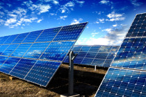
While many of us made New Year’s Resolutions on the eve of December 31 to ring in the New Year, last year’s celebration was also the heralding of a new era in lighting. January 1 marked the next phase in our government’s move to ban incandescent light bulbs in an effort to cut energy consumption. Last year, many retailers saw a jump in the sale of incandescent bulbs just prior to the start of phase 1. The fact that very few Canadians noticed this year’s changes signifies an acceptance that in many ways can be attributed to the improvements and growth in the LED sector.
One of the biggest obstacles in marketing LED technology to consumers is the cost, and while LED prices have been decreasing, many still cite the cost of the actual bulb as a deterrent despite the undisputed long-term savings (in both energy usage and cost). For now, LEDs are constructed two-dimensionally, or in a planar manner, in layers and are completely flat. Semi-conductor wafers are made to house even more layers of semiconductor crystals on it’s surface—a similar idea to baking a layer cake. The brighter the light, the more wafer area required, which means an increase in labour, and therefore, an increase in production costs. An exciting new research project funded by the European Commission under the 7th Framework Programme for Research and Technological Development has developed a new way to construct the way LEDs emit light by replacing the wafer with a “light emitting tower.”
The GECCO Project was initiated to run for three years, and concluded its research in 2015. Their goal was to “to develop white light emitting diodes (LEDs) with higher efficiency and lower cost per lumen than currently available.” The strategy to achieve this was to assemble LEDs three-dimensionally, so that each individual light bulb contained its own “light emitting tower.” The tower’s dimensions are within the micrometer range, which means an area of one square millimeter fits approximately one million LEDs—a precision only attained by applying nanotechnology manufacturing techniques. Since the surface area of an LED has more vertical area than horizontal, the tower increases the overall emitting area resulting in higher light output, avoiding some of the limitations of present nitrate material technology at a greatly reduced production cost. GECCO aimed to create a luminous efficacy of more than 200 lumens per watt, and while this efficacy was not achieved by the time the initiative concluded, their successful investigations have led to a new collaboration between two of GECCO’s original 6 partners, TUBS (Technische Universität Braunschweig) and OOS (OSRAM Opto Semiconductors GmbH). Implemented in 2014, and officially open in March 2015, the “Epitaxy Competence Center ec²” focuses on research that is application oriented in the field of nitride-based semiconductors within a multitude of technologies, including LED and Laser Technology. These technologies are essential mainstays in many areas: mechanical engineering, health care, and the automotive industry, to name a few. In fact, car headlights, LED lamps, and street lighting are all being designed based on nitrate-based white LED technology.
OOS CEO Aldo Kamper believes “Technological development towards even greater performance and lower cost of production has to go faster,” a sentiment we wholeheartedly agree with here at Mission LED Lighting. To find out how much you can save by making the switch to LEDs, check out LED Lights Canada’s Energy Savings Calculator, and make sure to keep checking back because we know it won’t be long before we’re blogging about “light emitting tower” LEDs stocking the shelves!
About The Author

-
Serial Entrepreneur, Technologist and Inventor.
My objective is to develop useful products that have a net positive effect in the lives of those that use them and the environment that we live in.
CEO of Mission LED Lighting Company Ltd.
- 2017.05.24LED factsWhy Are Cars Switching to LEDs if They’re Too Bright?
- 2017.05.09Be green & saveHow to Easily Replace T8 Fluorescent Tubes With LED
- 2017.03.07Build a better future7 Things About Explosion Proof LED Lighting You Should Know
- 2017.02.28Be green & saveWhy We Love LED Grow Lights (And You Should, Too!)

Leave a Reply